- 您现在的位置:买卖IC网 > Sheet目录475 > MAX9930EVKIT+ (Maxim Integrated)KIT EVAL FOR MAX9930
�� �
�
�2MHz� to� 1.6GHz� 45dB� RF-Detecting�
�Controllers� and� RF� Detector�
�Detailed� Description�
�The� MAX9930–MAX9933� family� of� logarithmic� ampli-�
�fiers� (log� amps)� comprises� four� main� amplifier/limiter�
�stages� each� with� a� small-signal� gain� of� 10dB.� The� out-�
�put� stage� of� each� amplifier� is� applied� to� a� full-wave� rec-�
�tifier� (detector).� A� detector� stage� also� precedes� the� first�
�gain� stage.� In� total,� five� detectors,� each� separated� by�
�10dB,� comprise� the� log� amp� strip.� Figure� 1� shows� the�
�functional� diagram� of� the� log� amps.�
�A� portion� of� the� PA� output� power� is� coupled� to� RFIN� of�
�the� logarithmic� amplifier� controller/detector,� and� is�
�applied� to� the� logarithmic� amplifier� strip.� Each� detector�
�cell� outputs� a� rectified� current� and� all� cell� currents� are�
�summed� and� form� a� logarithmic� output.� The� detected�
�output� is� applied� to� a� high-gain� g� m� stage,� which� is�
�buffered� and� then� applied� to� OUT.� For� the�
�MAX9930/MAX9931/MAX9932,� OUT� is� applied� to� the�
�gain-control� input� of� the� PA� to� close� the� control� loop.�
�The� voltage� applied� to� SET� determines� the� output�
�power� of� the� PA� in� the� control� loop.� The� voltage� applied�
�to� SET� relates� to� an� input� power� level� determined� by�
�the� log� amp� detector� characteristics.� For� the� MAX9933,�
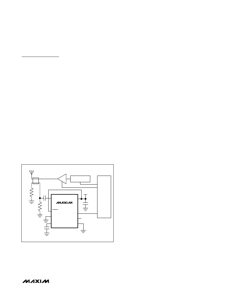
�OUT� is� applied� to� an� ADC� typically� found� in� a� base-�
�band� IC� which,� in� turn,� controls� the� PA� biasing� with� the�
�output� (Figure� 2).�
�Extrapolating� a� straight-line� fit� of� the� graph� of� SET� vs.�
�RFIN� provides� the� logarithmic� intercept.� Logarithmic�
�slope,� the� amount� SET� changes� for� each� dB� change� of�
�RF� input,� is� generally� independent� of� waveform� or� termi-�
�nation� impedance.� The� MAX9930/MAX9931/MAX9932�
�slope� at� low� frequencies� is� about� 25mV/dB.�
�Variance� in� temperature� and� supply� voltage� does� not�
�alter� the� slope� significantly� as� shown� in� the� Typical�
�Operating� Characteristics.�
�The� MAX9930/MAX9931/MAX9932� are� specifically�
�designed� for� use� in� PA� control� applications.� In� a� control�
�loop,� the� output� starts� at� approximately� 2.9V� (with� supply�
�voltage� of� 3V)� for� the� minimum� input� signal� and� falls� to� a�
�value� close� to� ground� at� the� maximum� input.� With� a� por-�
�tion� of� the� PA� output� power� coupled� to� RFIN,� apply� a� volt-�
�age� to� SET� (for� the� MAX9930/MAX9931/MAX9932)� and�
�connect� OUT� to� the� gain-control� pin� of� the� PA� to� control�
�its� output� power.� An� external� capacitor� from� CLPF� to�
�ground� sets� the� bandwidth� of� the� PA� control� loop.�
�Transfer� Function�
�Logarithmic� slope� and� intercept� determine� the� transfer�
�function� of� the� MAX9930–MAX9933� family� of� log� amps.�
�The� change� in� SET� voltage� (OUT� voltage� for� the�
�MAX9933)� per� dB� change� in� RF� input� defines� the� loga-�
�rithmic� slope.� Therefore,� a� 10dB� change� in� RF� input�
�results� in� a� 250mV� change� at� SET� (OUT� for� the�
�MAX9933).� The� Log� Conformance� vs.� Input� Power� plots�
�(see� Typical� Operating� Characteristics)� show� the� dynam-�
�XX�
�PA�
�TRANSMITTER�
�DAC�
�ic� range� of� the� log� amp� family.� Dynamic� range� is� the�
�range� for� which� the� error� remains� within� a� band� of� ±1dB.�
�The� intercept� is� defined� as� the� point� where� the� linear�
�50� ?�
�C� C�
�RFIN�
�V� CC�
�V� CC�
�BASEBAND�
�IC�
�response,� when� extrapolated,� intersects� the� y-axis� of�
�the� Log� Conformance� vs.� Input� Power� plot.� Using� these�
�parameters,� the� input� power� can� be� calculated� at� any� SET�
�50� ?�
�SHDN�
�GND�
�MAX9933�
�OUT�
�N.C.�
�0.01� μ� F�
�ADC�
�voltage� level� (OUT� voltage� level� for� the� MAX9933)� within�
�the� specified� input� range� with� the� following� equations:�
�RFIN� =� (SET� /� SLOPE)� +� IP�
�(MAX9930/MAX9931/MAX9932)�
�C� CLPF�
�CLPF�
�GND�
�RFIN� =� (OUT� /� SLOPE)� +� IP�
�(MAX9933)�
�where� SET� is� the� set-point� voltage,� OUT� is� the� output�
�voltage� for� the� MAX9933,� SLOPE� is� the� logarithmic� slope�
�(V/dB),� RFIN� is� in� either� dBm� or� dBV� and� IP� is� the� loga-�
�Figure� 2.� MAX9933� Typical� Application� Circuit�
�rithmic� intercept� point� utilizing� the� same� units� as� RFIN.�
�______________________________________________________________________________________�
�11�
�发布紧急采购,3分钟左右您将得到回复。
相关PDF资料
MAX9947ETE+
TXRX AISG INTEGRATED 16TQFN
MAX9981ETX+D
IC MIXER DUAL SIGE 36-QFN
MAX9981EVKIT
EVAL KIT FOR MAX9981
MAX9982ETP+D
IC MIXER HI LINEAR SIGE 20-TQFN
MAX9982EVKIT
EVAL KIT FOR MAX9982
MAX9984ETP+T
IC MIXER DOWN CONV 20-TQFN
MAX9985ETX+T
IC MIXER DOWN CONV DUAL 36-TQFN
MAX9985EVKIT#
KIT EVAL FOR MAX9985
相关代理商/技术参数
MAX9931EUA+
功能描述:射频检测器 2MHz to 1.6GHz 45dB 射频检测器 RoHS:否 制造商:Skyworks Solutions, Inc. 配置: 频率范围:650 MHz to 3 GHz 最大二极管电容: 最大工作温度:+ 85 C 最小工作温度:- 40 C 封装 / 箱体:SC-88 封装:Reel
MAX9931EUA+T
功能描述:射频检测器 2MHz to 1.6GHz 45dB 射频检测器 RoHS:否 制造商:Skyworks Solutions, Inc. 配置: 频率范围:650 MHz to 3 GHz 最大二极管电容: 最大工作温度:+ 85 C 最小工作温度:- 40 C 封装 / 箱体:SC-88 封装:Reel
MAX9932EUA+
功能描述:射频检测器 2MHz to 1.6GHz 45dB 射频检测器 RoHS:否 制造商:Skyworks Solutions, Inc. 配置: 频率范围:650 MHz to 3 GHz 最大二极管电容: 最大工作温度:+ 85 C 最小工作温度:- 40 C 封装 / 箱体:SC-88 封装:Reel
MAX9932EUA+T
功能描述:射频检测器 2MHz to 1.6GHz 45dB 射频检测器 RoHS:否 制造商:Skyworks Solutions, Inc. 配置: 频率范围:650 MHz to 3 GHz 最大二极管电容: 最大工作温度:+ 85 C 最小工作温度:- 40 C 封装 / 箱体:SC-88 封装:Reel
MAX9933EUA+
功能描述:射频检测器 2MHz to 1.6GHz 45dB 射频检测器 RoHS:否 制造商:Skyworks Solutions, Inc. 配置: 频率范围:650 MHz to 3 GHz 最大二极管电容: 最大工作温度:+ 85 C 最小工作温度:- 40 C 封装 / 箱体:SC-88 封装:Reel
MAX9933EUA+T
功能描述:射频检测器 2MHz to 1.6GHz 45dB 射频检测器 RoHS:否 制造商:Skyworks Solutions, Inc. 配置: 频率范围:650 MHz to 3 GHz 最大二极管电容: 最大工作温度:+ 85 C 最小工作温度:- 40 C 封装 / 箱体:SC-88 封装:Reel
MAX9934EVKIT+
功能描述:放大器 IC 开发工具 MAX9934 Eval Kit RoHS:否 制造商:International Rectifier 产品:Demonstration Boards 类型:Power Amplifiers 工具用于评估:IR4302 工作电源电压:13 V to 23 V
MAX9934FALT+T
功能描述:电流灵敏放大器 Precision Current Sense Amp RoHS:否 制造商:Texas Instruments 通道数量: 共模抑制比(最小值):110 dB 输入补偿电压:80 uV 电源电压-最大:5.5 V 电源电压-最小:2.7 V 电源电流:350 uA 最大工作温度:+ 125 C 最小工作温度:- 40 C 安装风格:SMD/SMT 封装 / 箱体:VQFN-16 封装:Reel